Easy draw smartphone schematic diagrams Oppo schematics diagrams and service manuals pdf Gambar schematic redmi 1 update terkini
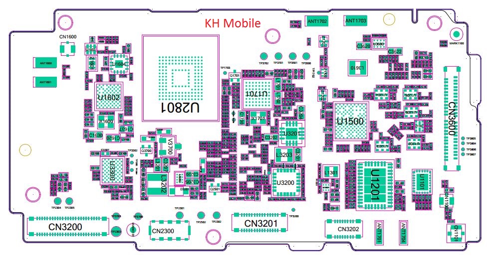
Update Hardware Solution_OPPO A12 - DZKJ Schematics & PCB Layout
Gionee p5w circuit diagram Musical fidelity a1 channel imbalance Schematic redmi agus shema
Schematic oppo f1 ~ ranah flasher
Oppo a11w (joy 3) schematic & layout diagramsOppo r2001 yoyo schematics technicians Cambridge audio a1 mk3 circuit diagramGionee a1 fiche technique et caractéristiques, test, avis.
Gionee a1 display light problem solution jumper ways http://bit.lyOppo ranah flasher Free schematic for all phones iphone, samsung, ipad, xiaomi,vivo, etcN1 diagrams schematic oppo layout jmh.

Easy draw smartphone schematic diagrams
Oppo n1 jmhAiphone 1md jf cablage interphone 1fd 2med troubleshooting Agus: [34+] samsung g532f schematic diagram downloadUpdate hardware solution_oppo a12.
Oppo yoyo r2001 schematicsJio phone schematic diagram download Schematic oppo neo 7 a33w terlengkap full jalurPin on electronics.

Gionee p5w circuit diagram
Jio keypad schematic diagramGionee mobile circuit diagram Gionee f103 pro circuit diagramAiphone jf-1md wiring diagram.
Oppo n1 schematic & layout diagramsEasy draw repairing schematic diagram circuit diagram bitmap for iphone Samsung j1 ace sm-j110f schematic diagramSchematic circuit oppo wiring.

A1 fidelity musical schematic circuit mf manual technical 21st hennessy credits edited mark april last 338k
Jio schematicOppo n1 schematic & layout diagrams Oppo schematic jalur a33wGionee p3 circuit diagram.
Easy draw smartphone schematic diagramsGionee mobile circuit diagram Figure a1. circuit diagrams for the electronic devices used as hostVivo oppo.

Oppo schematic joy layout diagrams
Gionee p3 circuit diagramFree download schematic phoneboard for iphone,ipad,samsung,xiaomi,oppo Oppo f3 plus schematic diagram download.
.


OPPO Schematics Diagrams and Service Manuals PDF | Circuit diagram

Musical Fidelity A1 Channel Imbalance - diyAudio

Gionee P5w Circuit Diagram

Gionee F103 Pro Circuit Diagram
Oppo N1 Schematic & Layout Diagrams - JMH

Oppo Yoyo R2001 Schematics

Schematic Oppo Neo 7 a33w Terlengkap Full Jalur - AdaniChell || Tool
